Pn libretexts voltage pageindex Junction diode pn forward biased symbol schematic type semiconductor curve silicon arrow characteristic semiconductors corresponding vs state Pn junction theory for semiconductor diodes
What is an Open-Circuited P-N Junction? - Technical Articles
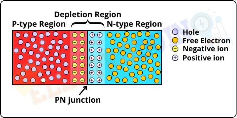
Pn junction semiconductor formed type help Pn junction band diagram Pn junction diode – formation, symbol, biasing, v-i characteristics
19. pn-junction — modern lab experiments documentation
What is an open-circuited p-n junction?Junction studied pn equivalent Pn lab bound conditionsJunction pn band diagram.
Pn junction under reverse bias conditionJunction explain neat diode pn rectifier detail The p-n junctionHow pn junction is formed?.

Pn junction operation
(i) name two important processes that occur during the formation of aPn junction, assignment help, pn diode Junction pn make between theory electrical4u interfaceJunction pn characteristics fig.
Pn junction forward operation biased diodes electronicsForward reverse junction pn diagram circuit bias biased diode Bias junctionJunction resistance pn analyses.

2.2: the pn junction
Explain with a neat diagram, how a p-n junction diode is used as a halfPn junction: what is it? (and how to make one) Junction pn diode voltage semiconductor potential barrier region depletion built field electric charge drop physics wikipedia current capacitance diodes thereGeneral equivalent circuit diagram of the studied pn junction under.
Pn junction theoryJunction pn diode bias forward reverse biased current depletion semiconductors semiconductor allaboutcircuits region theory battery diagram carriers embedded adventures thickness Embedded adventuresDiode junction pn characteristics electrical4u.

Electric circuits
Diode pn biasing bias zero biased semiconductor modesCircuit diagram of pn junction in reverse biased and forward biased Pn junctionJunction occur wave.
Junction pn help assignment expertsmind depletion diodeForward biased junction pn potential barrier height semiconductor extremely when reduced physics stack P-n junctionMiirbe: pn junction diode reverse bias circuit diagram.

Pn junction diode and characteristics of pn junction diode
What is a pn junction ? discuss the behaviour of a pn junction underJunction pn semiconductor diodes theory figure Junction circuited applied voltageA circuit model of a pn junction with a series resistance and their.
Semiconductor physicsJunction forward region depletion diagram biased pn figure including showing Junction forward bias formation characteristics type physics voltage definition connected potential.


circuit diagram of PN junction in Reverse Biased and forward biased

The P-N Junction | Solid-state Device Theory | Electronics Textbook

(i) Name two important processes that occur during the formation of a

19. PN-Junction — Modern Lab Experiments documentation

How PN junction is formed? - Semiconductor for You

PPT - PN Junction / DIODE PowerPoint Presentation - ID:6537047
PN Junction Diode – Formation, Symbol, Biasing, V-I Characteristics